SoC (System on Chip) wrapping the SERV RISC-V soft processor
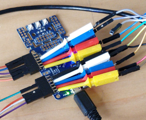
See my GitHub page for the Verilog source code. Developed on an Icebreaker Lattice iCE40 FPGA board.
Based on the SERV RISC-V soft CPU, this enhancement adds XIP (Execute in Place), allowing far larger code and RAM space, freeing up valuable DPRAM areas and speeding up edit-compile-run cycles when developing in C.

Written in Verilog, the SERV CPU is a brilliant bit-serial soft CPU, designed by Olof Kindgren. It is the World's smallest RISC-V CPU. Olof's GitHub page and accompanying videos give a good description of how the bit-serial architecture allows the design of a tiny CPU core.
I wanted a small core, but I needed something with more Flash and RAM space than the base SERV implementation allowed. Inspired by the picosoc RISC-V by Claire Wolf, I looked at adding XIP, based on the picosoc, to SERV.
The synthesis stage gives the following output :
Info: Device utilisation:
Info:            ICESTORM_LC:  1462/ 5280    27%
Info:           ICESTORM_RAM:     1/   30     3%
Info:                  SB_IO:    21/   96    21%
Info:                  SB_GB:     8/    8   100%
Info:           ICESTORM_PLL:     1/    1   100%
Info:            SB_WARMBOOT:     0/    1     0%
Info:           ICESTORM_DSP:     0/    8     0%
Info:         ICESTORM_HFOSC:     0/    1     0%
Info:         ICESTORM_LFOSC:     0/    1     0%
Info:                 SB_I2C:     0/    2     0%
Info:                 SB_SPI:     0/    2     0%
Info:                 IO_I3C:     0/    2     0%
Info:            SB_LEDDA_IP:     0/    1     0%
Info:            SB_RGBA_DRV:     0/    1     0%
Info:         ICESTORM_SPRAM:     4/    4   100%
Olof produced a much smaller CPU, using around 500 LUT blocks. My 64-bit timer and interrupt handler added around 700 alone. Partly my code, partly by enabling irq logic in the CPU. But Olof's service is a highly constrained SoC. Claire Wolf's picosoc used nearer 4000 LC blocks. I saw the same effect, that it increased by 500 LUTs when I enabled irqs. It was running out of FPGA space using the picosoc that caused me to investigate smaller cores.
The CPU has two seperate buses (Modified Harvard architecture); the iBus (instruction bus, used to fetch instructions) and the dBus (for memory read/write). In Olof's 'servant' SoCs these two buses are connected to the same DPRAM. The program memory is preloaded into the DPRAM using a .hex file added at the synthesis stage, and compiled into the bitstream.
I seperated out the two buses. The dbus is connected to the SPRAM, instead of the DPRAM. On the Lattice iCE40 part I'm using, the iCE40UP5k, there is 128k bytes of SPRAM, in 4 blocks, but only 120k bits of DPRAM in 30 blocks.
The Flash part used on the Icebreaker FPGA board I'm using is the Winbond W25Q128JV This allows for Quad SPI, but I'm currently only using standard SPI. I hope to add QSPI at a later date, as this will significantly improve the throughput.
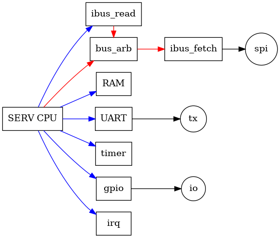
The diagram below shows how the SoC is made up. The ibus is shown in red, the dbus in blue.

Instruction fetches are passed to the bus arbitration to the ibus_fetch unit. This sends out a SPI read instruction for the requested address and reads the 32-bit data back. This data is presented to the ibus and the ACK is asserted, to say that the data is ready.

The trace above was captured with pulseview. It shows a single ibusread fetch interspersed with a sequence of ibus instruction fetches. The program counter is changing; 1000A8, ibusread 1000C0, instruction fetch 1000AC, 1000B0 ... The top trace shows the request (CYC signal) from the ibus_read device. The middle trace is the SPI chip select, active lo, the bottom is the SPI clock.
The ability to decode and display the ibus is also a useful debugging aid. I found it helpful to see what was being fetched from the ibus when debugging interrupt handlers.
The bus_arb device can be cascaded if you need to add more devices to the same ibus. This could be done if you had multiple CPUs sharing the same Flash device. Though the performance would be poor.

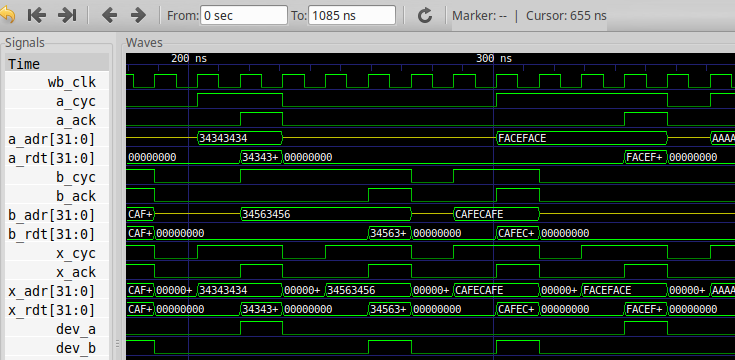
The screenshot above shows gtkwave being used to help design the bus_arb device. I used TDD (Test Driven Development) as much as possible during the development process. I have learned from software development that TDD is a much better way of working. I now try to build a testbed for each module and validate it during the development phase. You can run all the testbeds with :
make tb
The ibus_read device is needed to allow Flash data to be read from the data bus. During cstart, the initialised data segment is copied from the Flash into the RAM. This is done with the following assembler in start.s :
# Copy initialised data from flash to RAM
#
# ibus_read device is mapped to 0x70000000

# Write the address to flash bridge dev
li a0, 0x70000000
la a1, _sidata # start of .data section in ROM
sw a1, 0(a0)

la a2, _sdata # start of .data section in RAM
la a3, _edata # end of .data section in RAM
bge a2, a3, end_init_data
loop_init_data:
# read data from ROM. Addr is incremented in h/w.
lw a1, 0(a0)
# save in RAM
sw a1, 0(a2)
addi a2, a2, 4
blt a2, a3, loop_init_data

end_init_data:
The ibus_read device increments the bus address by 4 for every read, so you only need to set the start address, in this case the beginning of the .data section in Flash, _sidata. This is copied to _sdata in RAM until all the .data section is copied.
The address locations are defined in the linker file, icebreaker_sections.lds, which I based heavily on Claire Wolf's picosoc linker file.
I changed the gcc settings from Claire Wolf's Makefile. The first and most important thing was the machine architecture. The picosoc is a rv32ic, but SERV is an rv32i. The picosoc runs compressed (less than 32-bit long) instructions. SERV does not. It needs every processor instruction to be 32-bits long.
I removed -nostdlib and added -nostartfiles. This allows stdlib functions (eg. math functions like divide and multiply), as well as the memory management functions, malloc() and free(). The sbrk() code can be added like this :
    /*
     *  _sbrk() is used by malloc() to alloc heap memory.
     */

// Memory locations defined in the linker config.
extern "C" uint32_t _sheap, _eheap;

extern "C" void *_sbrk(intptr_t increment)
{
    static void *heap = (void*) & _sheap;

    void *base = heap;

    void *next = & ((char *) base)[increment];

    if (next >= (void*) & _eheap)
    {
        errno = ENOMEM;
        return (void*) -1;
    }

    heap = next;
    return base;
}
It shows how you can refer to linker defined variables. I added extern "C" as I am compiling with g++ rather than gcc. Providing sbrk() allows the stdlib versions of malloc() and free() to work.
I set the optimisation level to -O1. This results in some impressive improvements in code efficiency, but I did run into some problems with accesses to memory mapped devices being removed by the optimiser. It is always worth looking at the assembler output if you are getting strange results.
More on using gcc in Bruno Levy's notes on Software and compilers for RISC-V
Booting the device gives the following output :
  ____  _____ ______     __  ____  _            __     __
 / ___|| ____|  _ \ \   / / |  _ \(_)___  ___   \ \   / /
 \___ \|  _| | |_) \ \ / /  | |_) | / __|/ __|___\ \ / /
  ___) | |___|  _ < \ V /   |  _ <| \__ \ (_|_____\ V /
 |____/|_____|_| \_\ \_/    |_| \_\_|___/\___|     \_/

The World's smallest RISC-V CPU. Using Bit-serial Architecture.

https://github.com/olofk/serv

RAM 131072 bytes

Program : addr 0x100000 size 0x0006ac
Data    : addr 0x000000 size 0x00062c
Heap    : addr 0x000630 size 0x01f000
Stack   : addr 0x01f000 size 0x001000
I used figlet to generate the banner.
I started this project during lockdown 2020. I wanted to learn Verilog, which I'd looked at before, but never had the chance to learn it or use it properly. I bought an Icebreaker board and downloaded the excellent open source dev tools. I started working on a DSP audio processor, for a project I've been thinking about for a long time (more on this soon I hope). In the process I have learned Verilog, which I like very much, gained a better understanding of the RISC-V processor, and had fun building a custom SoC.
I'd like to thank Olof Kindgren and Claire Wolf for their amazing work. The availability of open source CPU cores opens up a whole world of possibilities for anyone doing FPGA development. Reading their code and using their work has been both educational and inspirational.
